— A Survey by Efthymios LallasORCIDGeneral Department of Lamia, University of Thessaly, 35100 Lamia, Greece
Appl. Sci. 2019, 9(24), 5488;
https://doi.org/10.3390/app9245488
Abstract
Wireless data traffic has experienced an unprecedented boost in past years, and according to data traffic forecasts, within a decade, it is expected to compete sufficiently with wired broadband infrastructure. Therefore, the use of even higher carrier frequency bands in the THz range, via adoption of new technologies to equip future THz band wireless communication systems at the nanoscale is required, in order to accommodate a variety of applications, that would satisfy the ever increasing user demands of higher data rates. Certain wireless applications such as 5G and beyond communications, network on chip system architectures, and nanosensor networks, will no longer satisfy speed and latency demands with existing technologies and system architectures.
Apart from conventional CMOS technology, and the already tested, still promising though, photonic technology, other technologies and materials such as plasmonics with graphene respectively, may offer a viable infrastructure solution on existing THz technology challenges. This survey paper is a thorough investigation on the current and beyond state of the art plasmonic system implementation for THz communications, by providing in-depth reference material, highlighting the fundamental aspects of plasmonic technology roles in future THz band wireless communication and THz wireless applications, that will define future demands coping with users’ needs.
Keywords: wireless NoC (WiNoC); graphene based WiNoCs (GWiNoCs); wireless nanosensor networks (WNSNs); surface plasmon polariton (SPP); GFET; multiple-input-multiple-output (MIMO); graphennas; THz transceiver
https://www.mdpi.com/2076-3417/9/24/5488
1. Introduction
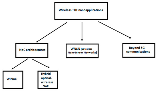
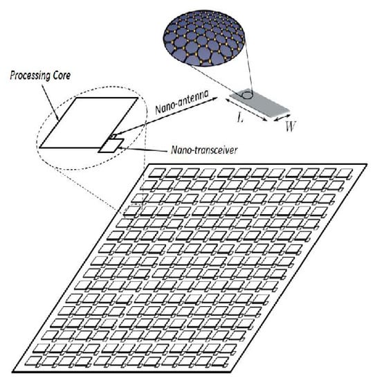
2. WiNoCs
2.1. WiNoC Architectures Potential